Let’s leave the conditional generator out of it for now…
This notebook was adapted from Ceviche’s inverse design introduction to use a JAX-based optimization loop in stead of the default Ceviche optimization loop.
Introduction: multi-mode waveguides
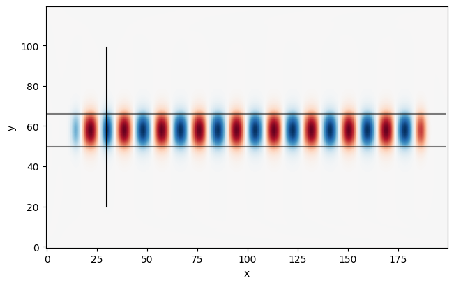
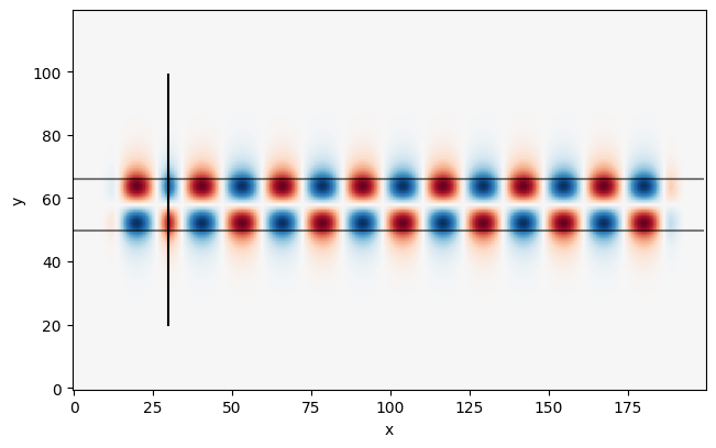
The ceviche package has a built-in method insert_mode() that allows different modes to be inserted as sources.
Below, we demonstrate how this functionality can be used to excite the first and second order modes of a straight waveguide:
# Define simulation parameters (see above)omega =2* np.pi *200e12dl =25e-9Nx =200Ny =120Npml =20# Define permittivity for a straight waveguideepsr = np.ones((Nx, Ny))epsr[:, 50:67] =12.0# Source positionsrc_y = np.arange(20, 100)src_x =30* np.ones(src_y.shape, dtype=int)# Source for mode 1source1 = insert_mode(omega, dl, src_x, src_y, epsr, m=1)# Source for mode 2source2 = insert_mode(omega, dl, src_x, src_y, epsr, m=2)# Run the simulation exciting mode 1simulation = ceviche.fdfd_ez(omega, dl, epsr, [Npml, Npml])Hx, Hy, Ez = simulation.solve(source1)# Visualize the electric fieldax = ceviche.viz.real(Ez, outline=epsr, cmap="RdBu_r")ax.plot(src_x, src_y, "k")# Run the simulation exciting mode 2simulation = ceviche.fdfd_ez(omega, dl, epsr, [Npml, Npml])Hx, Hy, Ez = simulation.solve(source2)# Visualize the electric fieldax = ceviche.viz.real(Ez, outline=epsr, cmap="RdBu_r")ax.plot(src_x, src_y, "k")plt.show()
Simulation and optimization parameters
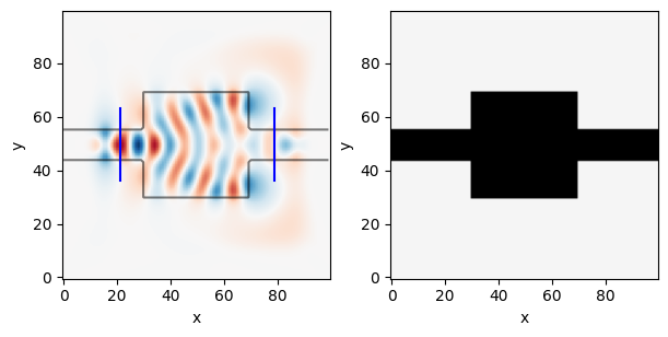
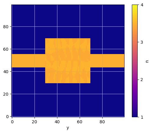
Our toy optimization problem will be to design a device that converts an input in the first-order mode into an output as the second-order mode. First, we define the parameters of our device and optimization:
# Angular frequency of the source in Hzomega =2* np.pi *200e12# Spatial resolution in metersdl =40e-9# Number of pixels in x-directionNx =100# Number of pixels in y-directionNy =100# Number of pixels in the PMLs in each directionNpml =20# Initial value of the structure's relative permittivityepsr_init =12.0# Space between the PMLs and the design region (in pixels)space =10# Width of the waveguide (in pixels)wg_width =12# Length in pixels of the source/probe slices on each side of the center pointspace_slice =8# Number of epochs in the optimizationNsteps =100# Step size for the Adam optimizerstep_size =1e-2
Utility functions
We now define some utility functions for initialization and optimization:
space : The space between the PML and the structure wg_width : The feed and probe waveguide width space_slice : The added space for the probe and source slices
Defines an overlap integral between the simulated field and desired field
Visualizing the starting device
We can visualize what our starting device looks like and how it behaves. Our device is initialized by the init_domain() function which was defined several cells above.
# Simulate initial devicesimulation, ax = viz_sim(epsr_total, source, slices=[input_slice, output_slice])# get normalization factor (field overlap before optimizing)_, _, Ez = simulation.solve(source)E0 = mode_overlap(Ez, probe)
Define objective function
We will now define our objective function. This is a scalar-valued function which our optimizer uses to improve the device’s performance.
Our objective function will consist of maximizing an overlap integral of the field in the output waveguide of the simulated device and the field of the waveguide’s second order mode (minimizing the negative overlap). The function takes in a single argument, epsr and returns the value of the overlap integral. The details of setting the permittivity and solving for the fields happens inside the objective function.
Returns the overlap integral between the output wg field and the desired mode field
Run optimization
This is where our discussion deviates from the original discussion by the ceviche maintainers. In our case, we would like the optimization to fit in a JAX-based optimization scheme:
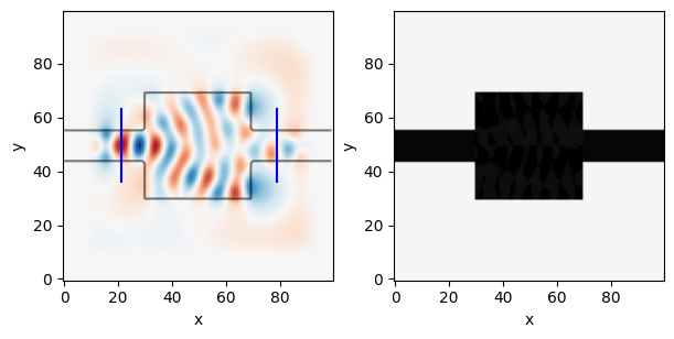
# Simulate and show the optimal deviceepsr_optimum_total = mask_combine_epsr(epsr_optimum, bg_epsr, design_region)simulation, ax = viz_sim(epsr_optimum_total, source, slices=[input_slice, output_slice])
At the end of the optimization we can see our final device. From the field pattern, we can easily observe that the device is doing what we intend: the even mode enters from the left and exits as the odd mode on the right.
However, an additional observation is that our device’s permittivity changes continuously. This is not ideal if we wanted to fabricated our device. We’re also not constraining the minimum and maximum values of \(\epsilon_r\). Thus, we need to consider alternative ways of parameterizing our device.